Researchers at the University of California, Berkeley, have developed an advanced method of growing nanolasers directly onto a silicon surface.
The next-gen process could lead to a new class of faster, more efficient microprocessors, as well as to powerful biochemical sensors that use optoelectronic chips.
“Our results impact a broad spectrum of scientific fields, including materials science, transistor technology, laser science, optoelectronics and optical physics,” explained UC Berkeley professor Connie Chang-Hasnain.
According to Chang-Hasnain, the increasing performance demands of electronic devices have prompted researchers to search for more efficient ways of harnessing the inherent ability of light particles – which are inherently capable of carrying far more data than electrical signals.
Indeed, optical interconnects are often seen as a solution to overcoming the communications bottleneck within and between computer chips.
Unfortunately, silicon – the material that forms the foundation of modern electronics – is extremely deficient at generating light.
As such, engineers are testing another class of materials known as III-V semiconductors to create light-based components such as light-emitting diodes (LEDs) and lasers.
Nevertheless, “marrying” III-V with silicon to create a single optoelectronic chip has thus far been somewhat problematic. For one, the atomic structures of the two materials are mismatched.
In addition, the manufacturing industry is understandably geared towards the production of silicon-based materials. For practical reasons, the goal has thus far been to integrate the fabrication of III-V devices into existing infrastructure.
“Today’s massive silicon electronics infrastructure is extremely difficult to change for both economic and technological reasons, so compatibility with silicon fabrication is critical,” said Chang-Hasnain.
“One problem is that growth of III-V semiconductors has traditionally involved high temperatures – 700 degrees Celsius or more – that would destroy the electronics. Meanwhile, other integration approaches have not been scalable.”
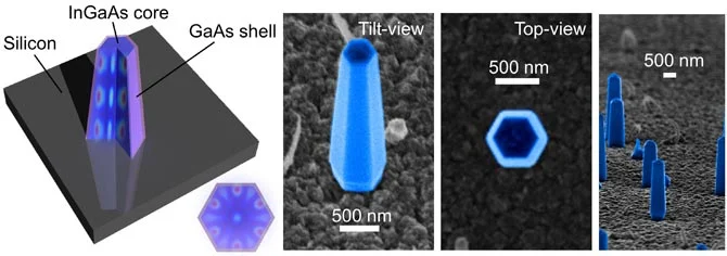
Still, UC Berkeley researchers managed to overcome this limitation by formulating a method of growing nanopillars made of indium gallium arsenide, a III-V material, onto a silicon surface at the relatively cool temperature of 400 degrees Celsius.
To accomplish this, researchers used metal-organic chemical vapor deposition to grow the nanopillars on the silicon. Once the nanopillar was made, the researchers demonstrated that it could generate near infrared laser light – a wavelength of about 950 nanometers – at room temperature.
The hexagonal geometry dictated by the crystal structure of the nanopillars creates a new, efficient, light-trapping optical cavity. Light circulates up and down the structure in a helical fashion and amplifies via this optical feedback mechanism.
As noted above, the unique approach of growing nanolasers directly onto silicon could lead to highly efficient silicon photonics.
To be sure, the miniscule dimensions of the nanopillars – smaller than one wavelength on each side, in some cases – make it possible to pack them into small spaces with the added benefit of consuming very little energy.
“Ultimately, this technique may provide a powerful and new avenue for engineering on-chip nanophotonic devices such as lasers, photodetectors, modulators and solar cells.
“This research has the potential to catalyze an optoelectronics revolution in computing, communications, displays and optical signal processing. In the future, we expect to improve the characteristics of these lasers and ultimately control them electronically for a powerful marriage between photonic and electronic devices,” added Chang-Hasnain.