The unique properties of graphene such as its incredible strength and, at the same time, its little weight have raised high expectations in modern material science.
Graphene, a two-dimensional crystal of carbon atoms packed in a honeycomb structure, has been in the focus of intensive research which led to a Nobel Prize of Physics in 2010. One major challenge is to successfully integrate graphene into the established metal-silicide technology.

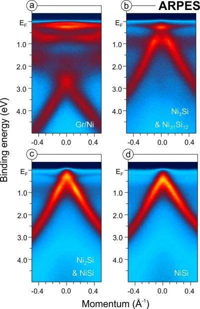
Scientists from the University of Vienna and their co-workers from research institutes in Germany and Russia have succeeded in fabricating a novel structure of high-quality metal silicides all nicely covered and protected underneath a graphene layer. These two-dimensional sheets are as thin as single atoms.
In order to uncover the basic properties of the new structure the scientists need to resort to powerful measurement techniques based on one of Einstein’s brilliant discoveries – the photoelectric effect. When a light particle interacts with a material it can transfer all its energy to an electron inside that material.
If the energy of the light is sufficiently large, the electron acquires enough energy to escape from the material. Angle-resolved photoemission spectroscopy (ARPES) enables the scientists to extract valuable information on the electronic properties of the material by determining the angle under which the electrons escape from the material.
“Single-atom thick layers and hybrid materials made thereof allow us to study a wealth of novel electronic phenomena and continue to fascinate the community of material scientists. The ARPES method plays a key role in these endeavours”, say Alexander Grueneis and Nikolay Verbitskiy, members of the Electronic Properties of Materials Group at the University of Vienna and co-authors of the study.
The graphene-capped silicides under investigation are reliably protected against oxidation and can cover a wide range of electronic materials and device applications. Most importantly, the graphene layer itself barely interacts with the silicides underneath and the unique properties of graphene are widely preserved.
The work of the research team, therefore, promises a clever way to incorporate graphene with existing metal silicide technology which finds a wide range of applications in semiconductor devices, spintronics, photovoltaics and thermoelectrics.


