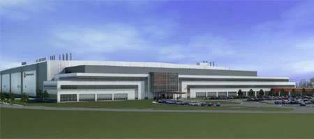
San Francisco (CA) – Globalfoundries has claimed that its future Fab 2 facility will allow the company “do more with less.” The fantastic fab – scheduled to be built in upstate NY – is expected to eliminate waste, reduce production time and lower inventory costs.
“Fab 2 will offer unique solutions and align production with customer demand,” Thomas Sonderman told reporters at Semicon 2009.
The VP of manufacturing systems and technology also noted that a “global workforce” with “indigenous capabilities” would help the corporation reach the next node “quickly” and with “lower costs.”
Jon Carvill of Globalfoundries expressed similar sentiments in an official blog post.
“Once constructed, we expect Fab 2 to be the world’s most advanced semiconductor foundry. Its construction represents more than three-years of careful planning and collaboration and an investment of roughly $4.2B,” wrote Carvill. “The technology in Fab 2 will be absolutely state of the art. Our current plan is to ramp it on 28nm technology in 2H 2012 and then make a quick transition to 22nm, in a similar fashion to what we did with Fab 36 for AMD in Dresden.”
Carvill also noted that Fab 2 “will come stacked with the latest generation” of APM software to ensure maximum automation, control and predictability.
“This is an industry unlike most in technology as it requires you to hedge significant and capital-intensive bets 3-5 years in advance. It’s the nature of the business and has been one of the key factors in driving consolidation over the past few years. More and more companies are moving to a fabless model and we expect that trend to continue,” added Carvill.