Malta (NY) – Globalfoundries, the spun-off manufacturing arm of AMD, provided a first glimpse at the plans of its 1.3 million square foot chip factory to be built at Luther Forest Technology Park in Saratoga County. The construction of the plant is still on schedule, but it will be more expensive than originally planned and technologically much more advanced: The factory will start production at 32 nm and the half-node 28 nm, but ramp quickly in 22 nm.
It has been almost three years since AMD unveiled its plans to build a chip factory to support its expansion. Back then, in June of 2006, AMD was flying high with its Opteron and Athlon X2 processors that took over market share from Intel almost at will. AMD’s market share gains were limited by its production capacity, especially with new customers such as Dell, and an expansion plan made sense. However, AMD underestimated Intel’s strength and ended up in huge debt, supported by the $5.4 billion acquisition of ATI, and some believe that the company remained only alive because Intel needs AMD to stay out of more antitrust trouble.
Globalfoundries is the result of AMD’s troubles, and has been created through $6 billion in committed investments from Abu Dhabi-based Advanced Technology Investment Company (ATIC), which holds 65.8% of the company. AMD holds the remaining 34.2% of the contract manufacturer. Globalfoundries currently has AMD as its sole customer, and runs its production in its Dresden, Germany-based fabs, now called Fab 1 Module 1 and Module 2 (formerly AMD Fab 30 and 36). Fab 2 will be built in the Luther Forest Technology Park, just outside Saratoga Springs, NY, on 223 acres of land.
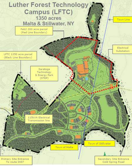
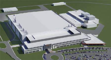
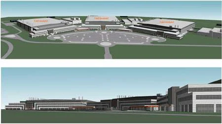
We recall that the original plans outlined a 1.2 million square foot building that would produce 32 nm processors and cost about $3.2 billion. Since 2006, those estimates have changed a bit – the building, which will begin construction this summer, will have more than 1.3 million square feet and cost about $4.5 billion, including land acquisition and production equipment. The fab will be larger than Intel’s largest fab, located in Kiryat Gat, Israel, and will have more floor space than the Chrysler building in New York City (1.2 million square feet). Globalfoundries said that it will take about 5 million man hours to build the first module of the fab. The fab itself will have about 883,000 square feet, while the clean room will measure about 300,000 square feet. AMD said that, at full production, the facility will be able to crank out about 35,000 wafers per month, which is more than the Dresden fabs, which have a capacity of 25,000 wafer starts each. Intel’s fabs are rumored to have a capacity of about 30,000 to 35,000 wafer starts per month each.
Globalfoundries recently showed the area of the future campus to journalists. There isn’t much to see yet, with the exception of streets and bike paths that were built as a contribution by the local government. Touring the Luther Forest Technology Park still requires a capable SUV in some areas. Globalfoundries has rented space in an office building within the Park, which will have space for about 35 employees for now. We were told that former AMD CEO and chairman and now Globalfoundries Chairman Hector Ruiz is present at the campus quite a bit, while the new investors from ATIC have remained in the (public) background so far.
What makes this new fab interesting is the fact that it is likely to be among the most advanced chip factory when it goes into full production 2012. Globalfoundries will be accepting 32 nm and 28 nm designs initially and ramp in 22 nm in 2012. If that plan will turn into reality, the manufacturer will be able to close the gap to Intel from today’s 12-18 months to a time frame that is closer to 6-9 months. And that achievement will be critical for the company to attract customers that compete with Intel. As the construction of new fabs will get more expensive (already today, only Intel and Samsung are the only semiconductor developers that are able to build working financial models around new chip plants) chip designers need to keep up with Intel and it would be a major advantage for Globalfoundries to stay close to its former rival, which now, at least in theory, could be a future customer. Globalfoundries said that it taped out first 32 nm SRAM silicon in Q4 2008 and will begin producing high-k metal gate chips in the first half of next year.
An interesting side note is the fact that the factory is located close to the University of Albany’s College of Nanoscale Science and Engineering (CNSE), which is considered the top school for chip development manufacturing in the United States. The school is trying to attract all the big names in chip manufacturing to research manufacturing techniques in the schools clean room facilities – right next to each other. And it appears that the idea is working very well, as the presence of companies such as IBM and Intel is business incentive enough for other companies to rent clean room space from the university.
There are massive investments taking place that other companies and students can take advantage of, such as Extreme Ultra Violet (EUV) chip printing systems – an immensely expensive technology that is now expected to become a reality at the 15 nm node. The school currently trains 160 grad students, who, by the way, do not pay for the education. The school pays a salary of about $25,000 per year and assumes the additional per-student cost of about $75,000 per year). It is a fascinating place to visit and if you are interested in seeing a chip factory from the inside, you should contact the CNSE staff, who gladly shows the facility especially to school classes.
For Globalfoundries, of course, the proximity to the CNSE is an advantage to enter partnerships to develop manufacturing techniques and recruit knowledgeable staff for its fabs closeby.
There is no lack of excitement for the future of the new company. And will certainly be interesting to see how the company will develop and which customers it can attract.