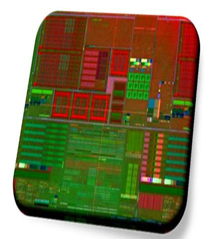
Globalfoundries is preparing for the next generation of mobile devices with the introduction of advanced 14nm-XM technology based on three-dimensional “FinFET” transistor architecture.
According to company spokesperson Jason Gorss, chips fabbed on the 14nm-XM process are expected to deliver a 40-60% improvement in battery life when compared to today’s two-dimensional planar transistors at the 20nm node.

“The XM stands for ‘eXtreme Mobility,’ and it is the industry’s leading non-planar architecture that is truly optimized for mobile system-on-chip (SoC) designs, providing a whole product solution from the transistor all the way up to the system level,” he explained.
Essentially, the 14nm-XM platform is based on a modular technology architecture that uses a 14nm FinFET device combined with elements of GloFo’s 20nm-LPM process.
“20nm-LPM technology enables a smooth transition for [those] looking to tap the benefits of FinFET SoCs as soon as possible,” said Gorss.
“Technology development is already underway, with test silicon running through Fab 8 in Saratoga County, N.Y. Early process design kits (PDKs) are [already] available, with customer tape-outs expected in 2013.”
For the uninitiated, FinFET architecture takes the traditional two-dimensional transistor design and turns the conductive channel on its side – resulting in a three-dimensional “fin” structure surrounded by a gate that controls the flow of current.
A key benefit of FinFET technology?
Its superior low-power attributes – as the 3D transistor design intrinsically operates at a lower voltage with minimal current leakage.
This translates into longer battery life for mobile applications or less power consumption for plugged-in applications such as networking chips in data centers.


