An international team of researchers has developed an artificial semiconductor structure capable of superimposing a pattern created by advanced fabrication methods that are precise at the nanometer scale.
The device, dubbed “artificial graphene” (AG), simulates quantum behavior of strongly interacting electrons.

Researchers believe the AG-device could be a “first step” towards the realization of an innovative class of solid-state quantum simulators to explore fundamental quantum physics.
Indeed, in order to study quantum phenomena, scientists typically employ artificial ad-hoc designed systems – quantum simulators – that can be controlled and manipulated in the laboratory.
However, the AG-device is the first quantum simulator to be based on a semiconductor material designed with the goal of uncovering quantum behavior of electrons.
“Quantum simulators based on novel artificial semiconductor structures are at the crossroads of quantum science and innovative technologies,” Professor Aron Pinczuk of Columbia University explained.
“While the frontiers of quantum physics are being explored with giant accelerators, in this branch of condensed matter science we employ advanced methods that expand the state-of-the-art in growth and processing of semiconductors. We could describe our work on quantum simulators as ‘probing quantum weirdness in a nano-nut-shell.'”
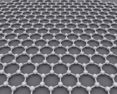
According to Pinczuk, the AG-device consists of a honeycomb lattice realized on the surface of a Gallium Arsenide (GaAs) heterostructure using advanced nanofabrication methods. The artificial honeycomb lattice structure replicates that of graphene, a material in which electrons behave in a peculiar way because of the crystal-lattice geometry.
With the ability to modify key parameters such as the lattice constant of the artificial lattice, scientists are now in a position to explore different regimes of electron-electron interactions in graphene-like systems.
The quantum simulator has already been tested with a “first run” trial that generated an unexpected peculiar quantum state. As such, researchers are understandably excited about the potential of creating venues for discovering novel quantum states which could, eventually, lead to new device concepts and eventually to an array of applications, for example, in advanced information processing or in cryptography.
“We hope next to achieve new breakthroughs through the creation of smaller nanofabricated structures reaching limits in which individual units in patterns have lengths of five nanometers,” said Pinczuk.
“This is [clearly] a state-of-the-art [project] that should open access to physics and materials science that has not yet been explored.”


