Graphite could help engineers in their perpetual quest to design smaller and more power efficient electronic devices.
Graphene – single sheets of graphite – measure only one atom thick, making it the world’s thinnest material. Indeed, two million graphene sheets stacked up wouldn’t even be as thick as a credit card.
However, physicists have yet to determine how to control the flow of electrons through the material, an obvious prerequisite for putting it to work in any type of electronic circuit.
Remember, graphene behaves very different than silicon, the material currently used in semiconductors.
Fortunately, a research team led by University of Arizona physicists managed to clear the first hurdle in 2011 by identifying boron nitride, a structurally identical but non-conducting material, as a suitable mounting surface for single-atom sheets of graphene.
The team also demonstrated that in addition to providing mechanical support, boron nitride improves the electronic properties of graphene by smoothening out fluctuations in electronic charges. Now the team has confirmed that boron nitride also influences how the electrons travel through the graphene – theoretically clearing the way for new methods of controlling the electron flow through graphene.
“For example, if you want to make a transistor, you need to be able to stop the flow of electrons,” said Brian LeRoy of the University of Arizona. “But in graphene, the electrons just keep going. It’s difficult to stop them.”
According to LeRoy, relativistic quantum mechanical effects that come into play at atomic scales cause electrons to behave in ways that are actually counterintuitive in terms of our expectations of how objects should act.
“Take tennis balls, for example. Normally, when you throw a tennis ball against a wall, it bounces back,” he explained. “Now think of the electrons as tennis balls. With quantum mechanical effects, there is a chance the ball would go through and end up on the other side. In graphene, the ball goes through 100 percent of the time.”
As LeRoy notes, this rather strange behavior makes it quite difficult to control where electrons are going in graphene. Nevertheless, mounting graphene on boron nitride can help prevent some of the electrons from passing to the other side – a first step toward a more controlled electron flow.
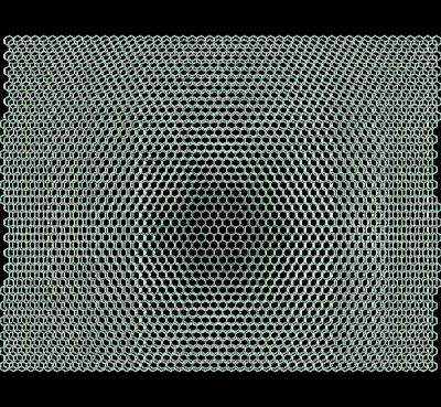
LeRoy’s team managed to achieve this feat by placing graphene sheets onto boron nitride at certain angles, resulting in the hexagonal structures in both materials to overlap in such a way that secondary, larger hexagonal patterns are created in the form of a superlattice.
If the angle is just right, they found, a point is reached where almost no electrons pass through.
“You could say we created holes in the wall. And as soon as the wall has holes in it, we find that some of the tennis balls no longer go through,” LeRoy noted. “Yes, It’s the opposite of what you would expect. That shows you how weird this is. It’s all due to those relativistic quantum effects.”
The above-mentioned discovery moves the technology somewhat closer to ultimately controlling the flow of electrons through the graphene.
“The effect depends on the size of the hexagonal pattern resulting from the overlapping sheets. The pattern creates a periodic modulation of the potential – picture a ball rolling across an egg carton,” explained LeRoy team member Matthew Yankowitz.
“It’s a purely electronic effect brought about by the structure of the two materials and how they sit on top of each other. It’s similar to the Moiré pattern you see when someone wears a striped shirt on TV.” Unfortunately, researchers are still unable to control how the graphene and boron nitride end up oriented relative to each other when they combine the two materials. Therefore, they make many samples and check the structure of each one under an electron microscope.
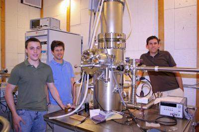
“With our scanning tunneling microscope, we can get an image of each superlattice and measure its size. We take a picture and see what the pattern looks like. If the hexagonal pattern is too small, the samples are no good and we throw them out… If it becomes possible to someday automate this process, graphene-based microelectronics might be well on their way to propel us from the silicon age to the graphene age,” he added.