Bending light beams to your whim sounds like a job for a wizard or an a complex array of bulky mirrors, lenses and prisms, but a few tiny liquid bubbles may be all that is necessary to open the doors for next-generation, high-speed circuits and displays, according to Penn State researchers.
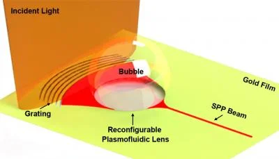
To combine the speed of optical communication with the portability of electronic circuitry, researchers use nanoplasmonics — devices that use short electromagnetic waves to modulate light on the nanometer scale, where conventional optics do not work. However, aiming and focusing this modulated light beam at desired targets is difficult.

“There are different solid-state devices to control (light beams), to switch them or modulate them, but the tenability and reconfigurability are very limited,” said Tony Jun Huang, associate professor of engineering science and mechanics. “Using a bubble has a lot of advantages.”
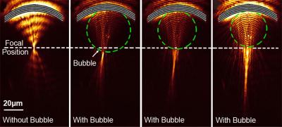
The main advantage of a bubble lens is just how quickly and easily researchers can reconfigure the bubble’s location, size, and shape — all of which affect the direction and focus of any light beam passing through it.
Huang’s team created separate simulations of the light beams and bubble lens to predict their behaviors and optimize conditions before combining the two in the laboratory. They published their findings in Nature Communications.

To form the bubble lens, researchers used a low-intensity laser to heat water on a gold surface. The tiny bubble’s optical behavior remains consistent as long as the laser’s power and the environmental temperature stay constant.


